- 您现在的位置:买卖IC网 > Sheet目录3889 > PIC16F1827-I/SS (Microchip Technology)IC PIC MCU FLASH 4K 20-SSOP
2011 Microchip Technology Inc.
DS41391D-page 13
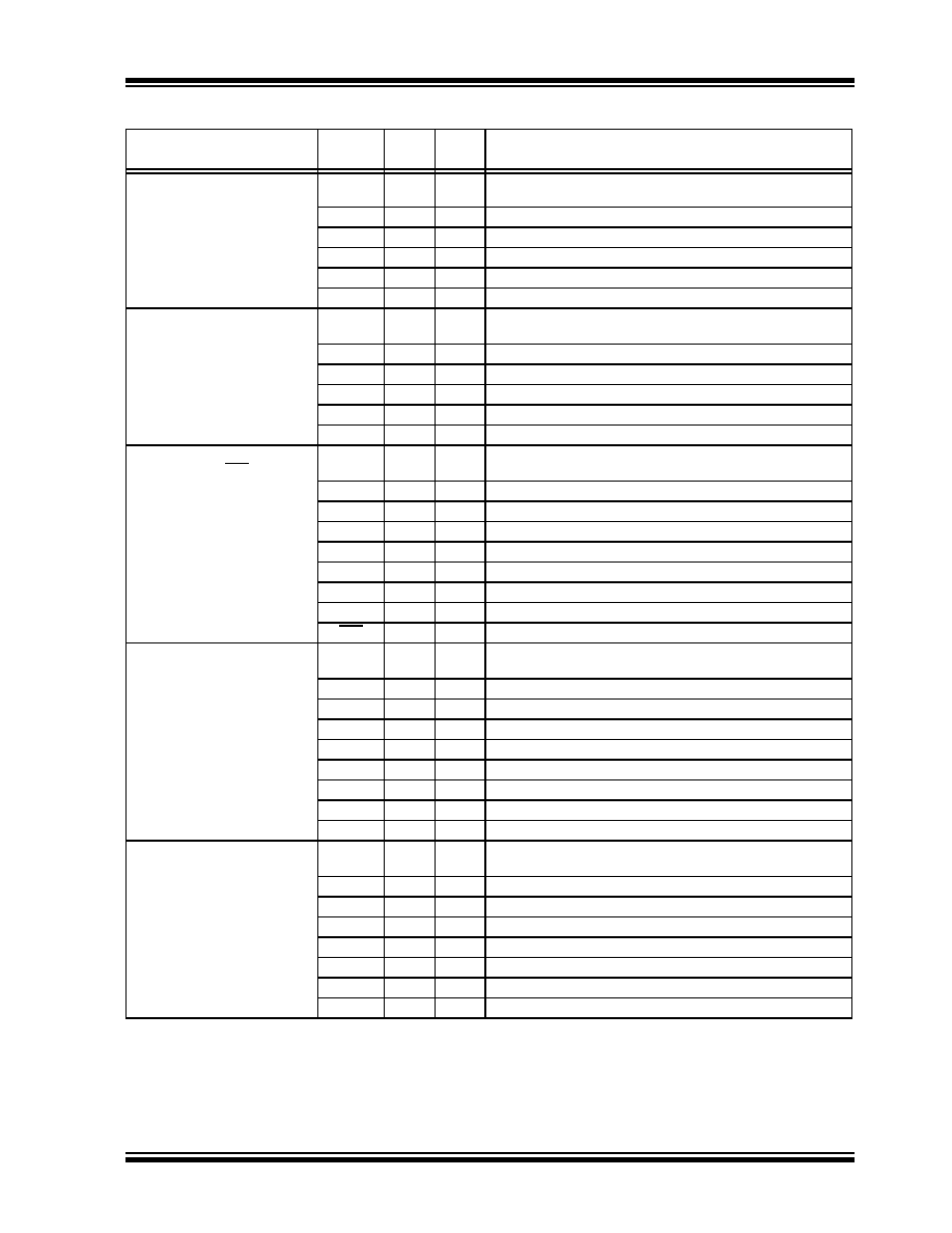
PIC16(L)F1826/27
RB3/AN9/CPS9/MDOUT/
CCP1(1,3)/P1A(1,3)
RB3
TTL
CMOS General purpose I/O. Individually controlled interrupt-on-change.
Individually enabled pull-up.
AN9
AN
—
A/D Channel 9 input.
CPS9
AN
—
Capacitive sensing input 9.
MDOUT
—
CMOS Modulator output.
CCP1
ST
CMOS Capture/Compare/PWM1.
P1A
—
CMOS PWM output.
RB4/AN8/CPS8/SCL1/SCK1/
MDCIN2
RB4
TTL
CMOS General purpose I/O. Individually controlled interrupt-on-change.
Individually enabled pull-up.
AN8
AN
—
A/D Channel 8 input.
CPS8
AN
—
Capacitive sensing input 8.
SCL1
I2C
OD
I2C clock 1.
SCK1
ST
CMOS SPI clock 1.
MDCIN2
ST
—
Modulator Carrier Input 2.
RB5/AN7/CPS7/P1B/TX(1)/CK(1)/
SCL2(2)/SCK2(2)/SS1(1,3)
RB5
TTL
CMOS General purpose I/O. Individually controlled interrupt-on-change.
Individually enabled pull-up.
AN7
AN
—
A/D Channel 7 input.
CPS7
AN
—
Capacitive sensing input 7.
P1B
—
CMOS PWM output.
TX
—
CMOS USART asynchronous transmit.
CK
ST
CMOS USART synchronous clock.
SCL2
I2C
OD
I2C clock 2.
SCK2
ST
CMOS SPI clock 2.
SS1
ST
—
Slave Select input 1.
RB6/AN5/CPS5/T1CKI/T1OSI/
P1C(1,3)/CCP2(1,2,3)/P2A(1,2,3)/
ICSPCLK
RB6
TTL
CMOS General purpose I/O. Individually controlled interrupt-on-change.
Individually enabled pull-up.
AN5
AN
—
A/D Channel 5 input.
CPS5
AN
—
Capacitive sensing input 5.
T1CKI
ST
—
Timer1 clock input.
T1OSO
XTAL
Timer1 oscillator connection.
P1C
—
CMOS PWM output.
CCP2
ST
CMOS Capture/Compare/PWM2.
P2A
—
CMOS PWM output.
ICSPCLK
ST
—
Serial Programming Clock.
RB7/AN6/CPS6/T1OSO/
P1D(1,3)/P2B(1,2,3)/MDCIN1/
ICSPDAT
RB7
TTL
CMOS General purpose I/O. Individually controlled interrupt-on-change.
Individually enabled pull-up.
AN6
AN
—
A/D Channel 6 input.
CPS6
AN
—
Capacitive sensing input 6.
T1OSO
XTAL
Timer1 oscillator connection.
P1D
—
CMOS PWM output.
P2B
—
CMOS PWM output.
MDCIN1
ST
—
Modulator Carrier Input 1.
ICSPDAT
ST
CMOS ICSP Data I/O.
TABLE 1-2:
PIC16(L)F1826/27 PINOUT DESCRIPTION (CONTINUED)
Name
Function
Input
Type
Output
Type
Description
Legend:
AN = Analog input or output CMOS= CMOS compatible input or output
OD
= Open Drain
TTL = TTL compatible input
ST
= Schmitt Trigger input with CMOS levels I2C = Schmitt Trigger input with I2C
HV = High Voltage
XTAL = Crystal
levels
Note 1:
Pin functions can be moved using the APFCON0 or APFCON1 register.
2:
Functions are only available on the PIC16(L)F1827.
3:
Default function location.
发布紧急采购,3分钟左右您将得到回复。
相关PDF资料
PIC12C508-04/P
IC MCU OTP 512X12 8DIP
22-15-3153
CONN FFC/FPC 15POS .100 RT ANG
PIC16F1826-I/MV
IC PIC MCU FLASH 2K 28-UQFN
PIC16F1825-I/P
MCU PIC 14K FLASH 1K RAM 14DIP
22-02-3153
CONN FFC/FPC VERTICAL 15POS .100
22-15-3143
CONN FFC/FPC 14POS .100 RT ANG
22-02-3143
CONN FFC/FPC VERTICAL 14POS .100
502078-2110
CONN FPC .25MM 21POS R/A SMD
相关代理商/技术参数
PIC16F1827T-I/ML
功能描述:8位微控制器 -MCU 7KB Flash 384 byte 32 MHz Int. Osc RoHS:否 制造商:Silicon Labs 核心:8051 处理器系列:C8051F39x 数据总线宽度:8 bit 最大时钟频率:50 MHz 程序存储器大小:16 KB 数据 RAM 大小:1 KB 片上 ADC:Yes 工作电源电压:1.8 V to 3.6 V 工作温度范围:- 40 C to + 105 C 封装 / 箱体:QFN-20 安装风格:SMD/SMT
PIC16F1827T-I/MQ
功能描述:8位微控制器 -MCU 7KB Flash 384 byte 32 MHz Int. Osc RoHS:否 制造商:Silicon Labs 核心:8051 处理器系列:C8051F39x 数据总线宽度:8 bit 最大时钟频率:50 MHz 程序存储器大小:16 KB 数据 RAM 大小:1 KB 片上 ADC:Yes 工作电源电压:1.8 V to 3.6 V 工作温度范围:- 40 C to + 105 C 封装 / 箱体:QFN-20 安装风格:SMD/SMT
PIC16F1827T-I/MV
功能描述:8位微控制器 -MCU 7KB Flash 384 RAM RoHS:否 制造商:Silicon Labs 核心:8051 处理器系列:C8051F39x 数据总线宽度:8 bit 最大时钟频率:50 MHz 程序存储器大小:16 KB 数据 RAM 大小:1 KB 片上 ADC:Yes 工作电源电压:1.8 V to 3.6 V 工作温度范围:- 40 C to + 105 C 封装 / 箱体:QFN-20 安装风格:SMD/SMT
PIC16F1827T-I/SO
功能描述:8位微控制器 -MCU 7KB Flash 384 byte 32 MHz Int. Osc RoHS:否 制造商:Silicon Labs 核心:8051 处理器系列:C8051F39x 数据总线宽度:8 bit 最大时钟频率:50 MHz 程序存储器大小:16 KB 数据 RAM 大小:1 KB 片上 ADC:Yes 工作电源电压:1.8 V to 3.6 V 工作温度范围:- 40 C to + 105 C 封装 / 箱体:QFN-20 安装风格:SMD/SMT
PIC16F1827T-I/SS
功能描述:8位微控制器 -MCU 7KB Flash 384 byte 32 MHz Int. Osc RoHS:否 制造商:Silicon Labs 核心:8051 处理器系列:C8051F39x 数据总线宽度:8 bit 最大时钟频率:50 MHz 程序存储器大小:16 KB 数据 RAM 大小:1 KB 片上 ADC:Yes 工作电源电压:1.8 V to 3.6 V 工作温度范围:- 40 C to + 105 C 封装 / 箱体:QFN-20 安装风格:SMD/SMT
PIC16F1828-E/ML
功能描述:8位微控制器 -MCU 7 KB Flash 256b RAM 32 MHz Int. Osc RoHS:否 制造商:Silicon Labs 核心:8051 处理器系列:C8051F39x 数据总线宽度:8 bit 最大时钟频率:50 MHz 程序存储器大小:16 KB 数据 RAM 大小:1 KB 片上 ADC:Yes 工作电源电压:1.8 V to 3.6 V 工作温度范围:- 40 C to + 105 C 封装 / 箱体:QFN-20 安装风格:SMD/SMT
PIC16F1828-E/P
功能描述:8位微控制器 -MCU 7 KB Flash 256b RAM 32 MHz Int. Osc RoHS:否 制造商:Silicon Labs 核心:8051 处理器系列:C8051F39x 数据总线宽度:8 bit 最大时钟频率:50 MHz 程序存储器大小:16 KB 数据 RAM 大小:1 KB 片上 ADC:Yes 工作电源电压:1.8 V to 3.6 V 工作温度范围:- 40 C to + 105 C 封装 / 箱体:QFN-20 安装风格:SMD/SMT
PIC16F1828-E/SO
功能描述:8位微控制器 -MCU 7 KB Flash 256b RAM 32 MHz Int. Osc RoHS:否 制造商:Silicon Labs 核心:8051 处理器系列:C8051F39x 数据总线宽度:8 bit 最大时钟频率:50 MHz 程序存储器大小:16 KB 数据 RAM 大小:1 KB 片上 ADC:Yes 工作电源电压:1.8 V to 3.6 V 工作温度范围:- 40 C to + 105 C 封装 / 箱体:QFN-20 安装风格:SMD/SMT